
:cheesygri
http://www.blachford.info/computer/articles/CellProgramming3.html
http://www.blachford.info/computer/articles/CellProgramming2.html
http://www.blachford.info/computer/articles/CellProgramming1.html
http://www.osnews.com/story.php?news_id=14969
http://www.blachford.info/computer/Cell/Cell0_v2.html
http://www.blachford.info/computer/Cell/Cell4_v2.html
http://www.blachford.info/computer/Cell/Cell1_v2.html
http://www.blachford.info/computer/Cell/Cell3_v2.html
http://www-128.ibm.com/developerworks/power/library/pa-cell/
-----------------------------------
Code:
skip to main content

developerWorks  >  Power Architecture technology | Linux  >
Spufs: The Cell Synergistic Processing Unit as a virtual file system

The Linux programming model for Cell
	developerWorks


Document options
	Set printer orientation to landscape mode

Print this page
	Email this page

E-mail this page

Free download:


Using Apache Tomcat but need to do more?

Rate this page


Help us improve this content

Level: Intermediate

Arnd Bergmann (arnd@arndb.de), Kernel Hacker, Linux on Cell kernel maintainer, IBM Deutschland Entwicklung GmbH

25 Jun 2005

    Base platform support for Linux on the Cell has been established and is currently on its way into the mainstream Linux kernel tree. Read about the Cell's unique architecture and the SPU file system interface that allows Linux to run on it.


More dW content related to: programming for CELL processor


    This article is adapted from the paper The Cell processor programming model presented at LinuxTag 2005; see the Resources section for more details.

The Cell processor from Sony, Toshiba, and IBM® is this year's most awaited newcomer on the CPU market. It promises unprecedented performance in the consumer and workstation market by employing a radically new architecture. Built around a 64-bit PowerPC® core, multiple independent vector processors called Synergistic Processing Units (SPUs) are combined on a single microprocessor.

Unlike existing SMP systems or multicore implementations of other processors, on the Cell, only the general purpose PowerPC core is able to run a generic operating system, while the SPUs are specialized to run computational tasks. Porting Linux™ to run on Cell's PowerPC core is a relatively easy task because of the similarities to existing platforms like IBM pSeries® or Apple Power Macintosh, but this does not give access to the enormous computing power of the SPUs.

Only the kernel can directly communicate with an SPU and therefore needs to abstract the hardware interface into system calls or device drivers. The most important functions of the user interface include loading a program binary into an SPU, transferring memory between an SPU program and a Linux userspace application, and synchronizing the execution. Other challenges are the integration of SPU program execution into existing tools like GDB or OProfile.

A joint team of Sony, IBM, and Toshiba employees based in Austin, Texas, did the groundwork for the Linux kernel port. The current set of kernel patches is based on the latest 2.6.xx snapshot kernel and is maintained by the IBM LTC (Linux Technology Center) team in Böblingen, Germany. The team hopes to integrate most of this into the 2.6.13 kernel release so it will become part of upcoming distribution releases.

The Cell processor

PowerPC Processing Element

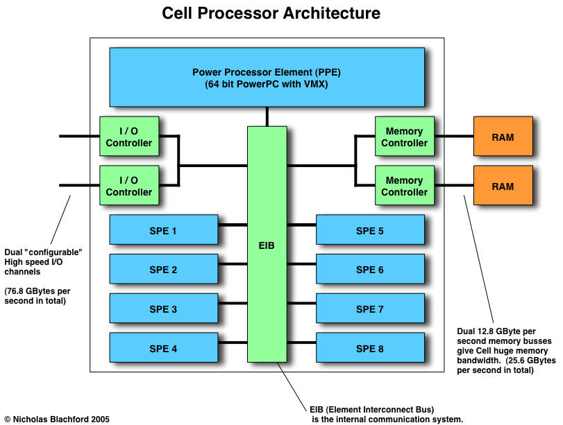
The Cell processor has a PowerPC Processing Element (PPE) that follows the 64-bit PowerPC AS architecture, as the PowerPC 970 CPU (also known as the G5) and all recent IBM POWER™ processors also use. Like the 970, it can use the VMX (AltiVec) vector instructions to parallelize arithmetic operations.

Moreover, the Cell processor can use simultaneous multithreading (SMT) like the IBM POWER5™ processor or Intel®'s Pentium 4 processors with Hyperthreading.

The IBM LTC has a standard Linux distribution running on the PPE and needs only a small number of kernel patches to add support for some of the hardware features that differ from existing target platforms. In particular, the Cell processor includes an interrupt controller and an IOMMU implementation, both of which are incompatible with those supported by older kernel versions.

The hardware we are running on at the LTC is a prototype of the Cell processor-based Blade, with two Cell processors running as a symmetric multiprocessing (SMP) system and, currently, 512MB of memory. It is designed to be used in an IBM BladeCenter™ chassis.

The integration of support for the PPE in one of the next kernel releases will enable the use of a single kernel binary for all current 64-bit PowerPC machines including Cell, Apple Power Mac, and IBM pSeries.

While no plans are in place to support 32-bit Linux kernels on Cell, it is possible to run both 32- and 64-bit distributions on it using the PowerPC 64 kernel with support for the ELF32 binary format. Note that all 32-bit PowerPC applications are expected to work without modifications.


	Back to top


Synergistic Processing Elements

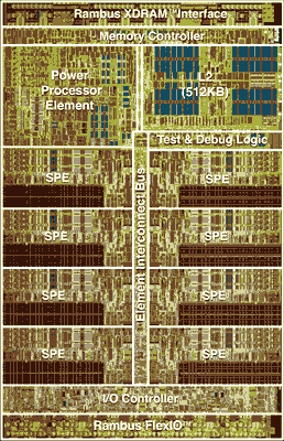
The Synergistic Processing Elements (SPEs) are the most interesting feature of the Cell processor, as they are the source of its overwhelming processing power. A single chip contains eight SPEs, each with an SPU, a Memory Flow Controller (MFC), and 256KB of SRAM that are used as local store memory.

An SPU uses vector operations itself and can thereby execute up to eight floating point instructions per clock cycle.

Bus interfaces

The Cell processor has three high-speed bus interfaces, one for memory and two for I/O or SMP connections. The memory interface connects XDRAM chips, which currently is the fastest available memory technology, substantially faster than current DDR or DDR2 interfaces.

Like the memory interface, the other two interfaces are also based on Rambus technology. One of them is used exclusively to connect I/O devices, typically a south bridge or north bridge chip for the FlexIO protocol. The other one can also be used for I/O, or alternatively as a coherent interface to connect multiple Cell processors to an SMP system.

Basic SPU design

An SPU resembles a cross between a simple CPU design and a digital signal processor. It can use the same instructions to do either 32-bit scalar or 128-bit vector processing. It has an 18-bit address space that accesses 256KB of local store that are part of the chip itself. Neither a memory management unit nor an instruction or data cache are used. Instead, the SPU can access any 128-bit word in the local store at L1 cache speed.

Memory Flow Controller

The MFC is the main communication vehicle between the local store memory and the system memory. As mentioned before, there is one MFC in each SPE. It has an integrated memory management unit that is normally used to provide access to the address space of one process by using the same page table lookup as the PPE.

A DMA request always involves moving data between the SPE local store and a virtual address space on the PPE side. The types of DMA requests include aligned read and write operations as well as single word atomic updates that can be used -- for example -- to implement spin-locks that are shared between SPEs and user processes.

Both the SPE and the PPE can initiate DMA transfers. The PPE does this through memory-mapped register access from kernel mode, while the SPE writes to its DMA channels from code running on the SPU.

An MFC can have multiple concurrent DMA requests to one address space outstanding from both the PPE and the SPU. Each MFC can access a separate address space.


	Back to top


Instruction set

Programs running inside the SPU need to be rather simplistic and self-contained, so you don't need complicated access protection or different privilege modes in the SPU itself. As a consequence, the instruction set contains mostly arithmetic and branch operations but none that resemble kernel mode instructions of the PPE.

Also, exceptions resulting from executed code aren't reported to the SPU itself. If a serious error occurs, for example, an invalid opcode, the SPU is stopped and an interrupt is delivered to the PPE. Some of the common sources of exceptions are not even possible on the SPU. For example, there are no addressing exceptions since all pointers get aligned and truncated to the local store size when attempting a memory access.

The arithmetic vector operations are similar to the VMX operations of the PPE, and you can use them for highly optimized video, image processing, or scientific applications, among others.

The main communication method of the SPU with other parts of the Cell processor is defined by a number of "channels." Each channel has a predefined function and is either a read channel or a write channel.

For example, a mailbox mechanism is a basic communication method between the SPE and the PPE. The SPU has a read channel for receiving a single data word from the mailbox and two write channels for sending data words (more on this below). One of those write channels is defined to generate external interrupts on the CPU when data is available, and the other does not have a notification mechanism.

When an SPU tries to read from an empty mailbox, it will stop execution until some value is written to its memory-mapped register.

When the PPE wants to access the mailbox, it needs to have access to the memory-mapped register space, which is normally only available to kernel space. It has three mailbox registers for each SPU, and each of those accesses one of the three SPU mailbox channels.

The memory-mapped registers are used by the PPE to control certain aspects of an SPE, but are not accessible by the SPU code itself. For example, one PPE-side mailbox register appears as a write-only physical memory location. When the PPE writes a data word to that address, the SPU can read from its corresponding mailbox read channels.

Other channels are used to access virtual memory associated with a user context on the PPE. By writing to DMA channels, the SPE can initiate a memory transfer, which is executed in parallel to both the SPU code execution and the PPE control flow. Only when a page fault is hit, for example, because the accessed page has been swapped out to disk, does the PPE receive an interrupt.


	Back to top


Possible programming models

Character devices

Some kernel code is needed to use the SPUs from a Linux application, since the controlling registers are only accessible from the PPE in privileged mode. The simplest way to give userspace applications access to hardware resources is through a character device driver controlled through read, write, and ioctl system calls.

This is suitable for many simple devices and at some point was used for testing the capabilities of the processor, but the approach has a number of problems. Most importantly, if each SPU is represented by a single character device, it becomes hard for an application to find an SPU that is not yet used by another. Moreover, that interface does not allow virtualization of the SPUs on a multiuser system in a sane way.

System calls

A different approach to using SPUs is to define a set of system calls. This makes it possible to replace physical SPUs as the underlying unit of the abstraction from processes running on the SPU. SPU processes can be scheduled by the kernel, and all users can create them without interfering with each other. On the downside, this also means duplicating some infrastructure of the kernel as well as adding a potentially large number of new system calls to provide all necessary functionality.

For example, when a new thread ID space is managed next to the existing Linux process IDs, substantial changes to all system calls dealing with PIDs (kill, getpriority, ptrace, and so on), or alternatively new versions of those system calls, need to be provided. Neither-------------------------------
cell از کلاس های استاندارد زبون سی و سی پی پی استفاده میکنه

آخرین ویرایش:


